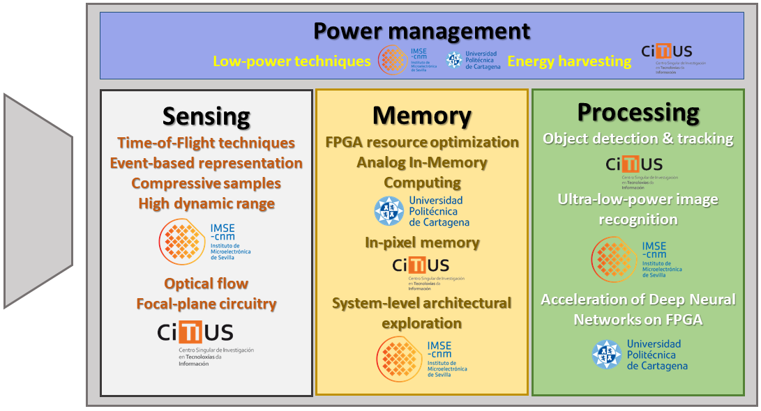
The general objective of this project is to conceive and develop vision systems proving that a holistic approach achieves much higher impact at application level than following closed and separated specifications per component. Our research will be transdisciplinary, encompassing elements along the entire visual signal chain. We will explore new sensing strategies, circuit structures, architectural arrangements, processing algorithms, dataflow optimization mechanisms, memory schemes, low-power techniques etc. This is summarized in the figure below, in which we have divided a generic vision system in four primary research areas: Sensing, Memory, Processing and Power Management. The conventional approach when designing such a system consists in mapping these areas into independent design blocks. The requirements per block are set without further consideration about the impact of fixed parameters at one level on critical parameters at other levels. The core of the innovation in this project is the departure from this conventional scheme.
In order to achieve the general objective defined above, we will target the following specific objectives per team in this coordinated project:
Specific objectives of IMSE’s project
1. A smart image sensor prototype exploiting the concurrency of light intensity and direct time-of-flight detection in CMOS. This sensor will be based on single-photon avalanche diodes (SPADs) and will provide the means for photon counting and timestamping. It will be designed in a CMOS image sensor technology, like LFoundry 110nm (LFoundry is about to become partner organisation of project ACHIEVE). Estimation of the time-of-flight will have a resolution around 100ps, which corresponds to 3cm distance. The image size will be 160 x 120 pixels.
2. Implementation of an embedded vision system with a maximum volume of 25cm3 and a maximum weight of 100g; it will operate at video rate, that is, 30 images per second, with a minimum resolution of 640 x 480 pixels (VGA); its energy efficiency will be below 50nJ per pixel, being able to recognize objects among at least 100 categories with an accuracy (top-1) of 80%.
3. The on-chip generation of alternative representations of the scene based on the extraction of characteristics at the image plane. We will exploit the relative lightness of the description of the scene in certain reference basis. We will develop a prototype smart image sensor chip with 320 x 240 pixels and the infrastructure for feature extraction at 30-60fps. It will be fabricated in LFoundry 110nm.
4. Design of a holistic simulator of vision systems encompassing performance parameters at sensor, memory, processing and power management levels. This simulator will be remotely accessed by researchers through the Internet. It will allow to globally assess the impact of specific parameters on application-level requirements through various figures of merit. Likewise, it will be flexible enough to define new evaluation metrics for further analysis. In addition to raw data, the simulator will output dynamic graphical representations of the exploration domain.
5. Generation of a DNN for image recognition tailored for deployment in embedded systems. This DNN will result from a training stage that will take into account usual constraints in battery-operated devices, e.g. memory, computational load and image resolution. We specifically aim at a DNN capable of recognizing 20 categories, demanding less than 100kBytes of memory for inference on 64x64-px images with an accuracy (top-1) of 70%.
Specific objectives of CiTIUS-USC’s project
1. Implementation of the Aggregated Local Flow Descriptor (ALFD), which integrates FAST and optical flow features, on a CMOS vision sensor in CMOS Imaging Sensor (CIS) technology. We aim at QVGA (320 x 240) resolution with a frame rate above 30 fps, and less than 250 mW of power consumption.
2. Implementation of a multi-target tracking system on a high-performance computing embedded GPU. This system will be oriented to the two main objects of interest in traffic monitoring, namely pedestrians and vehicles. It will integrate a state-of-the-art object detector algorithm based on Deep Learning, with trackers top-ranked in international challenges on standard benchmarks, e.g. Visual Object Tracking (VOT) and/or Multiple Object Tracking (MOT). The targeted system will run at least at 25 frames per second for more than 6 hours on a 6000 mA x h battery.
3. Implementation of an on-chip power management unit (PMU) based on capacitive DC/DC converters. This unit will provide several regulated output voltage levels for a dual-mode CMOS vision sensor with energy harvesting and processing capabilities. We aim at an efficiency over 50% for a power output in the range of nW - mW.
4. Implementation of a dual-mode CMOS vision sensor in CMOS Imaging Sensor (CIS) technology. This sensor will work as a self-powered sensor with background subtraction to perform tracking by detection. We aim at breaking state-of-the-art metrics, i.e. a chip with self-sustained operation reaching 15 fps with 60 klux in imaging mode.
Specific objectives of UPCT’s project
1. Define a methodology to evaluate, at system level, the optimal mapping of a DNN on embedded vision systems consisting of both digital and mixed-signal sections. We will consider a prescribed set of specifications defined in terms of frame rate, image size, hardware resources and power dissipation. We will focus on gray level image sequences having resolutions ranging from 64x64 to 320x240 pixels.
2. Design and synthesis of an ASIC on CMOS standard technology that integrates mixed-signal operators in order to assess the effect of such alternative processing structures on prescribed design parameters including power consumption and throughput. We will focus on multiply and carry (MAC) operations, which support most of the workload in DNNs. As a reference, the operators should perform multiplications of 4-bit analogue values to provide a digital output in a single clock cycle with less than 250 fJ of energy consumption.
3. Synthesis at register level (VHDL) of hardware-oriented architectures for embedded vision systems based on DNNs. We will apply reduced precision algorithms and datapath optimization for a tracking-by-detection algorithm. The input to the DNN will be data resulting from a lightweight representation of visual information rather than raw images. To this end, we will make the most of the analog-to-information conversion performed at the focal plane. The frame rate will be 30 fps for image sizes up to 320x240 pixels.
4. Synthesis on FPGA, training and test of the tracking-by-detection algorithm. The training of the network will be done on GPUs. The results achieved by the inference will be analyzed to correct the deviations with respect to the behavioural description. This objective ends with the deployment of a real demonstrator working at real time.